SystemX Affiliates: login to view related content.

Receiver architectures and circuits for the 5G technologies will be reviewed in this presentation. Two possible architectural directions towards 5G are considered.
From the SNR point of view, we can think of the sensitivity radio (or the long-distance radio) as the one extreme, and the maximum throughput radio (or the short-distance radio) as another extreme.
From the technology point of view, we can think of the co-working cellular radio (or the 3G/4G/4G+ radio) as the one extreme, and the co-working connectivity-cellular radio (4G+/WLAN radio) as another extreme.
All these cellular and connectivity technologies ‘speak’ different standardization languages, but from the RF IC design point of view there are many similarities that could be used to build a universal radio working across all the SNRs, distances, throughputs, and technologies from the very same circuits. In this presentation, the receiver architectures and circuits meeting this common goal of ‘all-in-1’ radio will be put up for a consideration.
An ‘imaginary’ local very-high throughput personal network (radio-belt) is introduced as a vehicle to build a 5G system with a 10Gb/s data rate. Design trade-offs among different modulation schemes, bandwidths, bands, and MIMO and beamforming signal-processing techniques are discussed throughout the presentation and their impact on the 5G circuit and architecture design outlined.
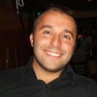
Dr. Tasic has over 15 years of experience in the field of RF IC design for multi-standard multi-band multi-mode and adaptive circuits and systems for wireless communications.
Dr. Tasic got his PhD from the Delft University of Technology, the Netherlands, in 2005, and worked afterwards as an Assistant Professor at the Delft University of Technology and a Visiting Scientist at the University of California San Diego until 2007. Since 2007 he’s been with Qualcomm San Diego as a Senior, Staff, and Senior-Staff Design Engineer, and Senior-Staff and Principal Manager. Between 2014-2015 he was with Mediatek San Diego as a Deputy Technical Director of the RF IC design team working on the advanced multi-carrier cellular transceivers.
Dr. Tasic worked on the world's 1st 4G transceiver and the world’s lowest-consumption 4G transceiver in the 2nd generation. He led a receive design team towards the world's 1st transceiver for carrier aggregation supporting simultaneous operation of multiple receivers.
Dr. Tasic laid down the IP groundwork for the expandable carrier-aggregation transceivers interfacing the external front-end amplifier modules and other transceivers whereby enabling seamless aggregation of carriers and enhanced sensitivity and throughput performance.
He patented the key carrier aggregation circuits and transceiver architectures implemented in more than 2 billion transceivers that are shipped to the leading phonemakers. He holds 14 patents and 26 patent submissions. Dr. Tasic was an Associate Editor for TCAS-I between 2010-2012. He published more than 30 conference and journal papers and 2 books.


