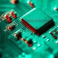

This next phase of semiconductor discovery will transcend electrical engineering and involve many other academic disciplines. | Stocksy/PER Images
Found in virtually every gadget powered by batteries or electricity, so ubiquitous as to be taken for granted, is that bedrock of our technological era, the semiconductor chip.
But last year, when automotive assembly lines stalled for lack of chips to build everything from anti-lock brakes to automatic door locks, public officials began to recognize the crisis that research and industrial scientists had seen coming.
“The world isn’t just facing production shortages for the chips we rely on today,” said Stanford electrical engineering Professor H.-S. Philip Wong. “We aren’t moving fast enough to create the next generation of semiconductors that we’ll need to broaden educational and economic opportunities, conserve energy and natural resources, and provide better and fairer access to technology.”
That sense of urgency and excitement suffused a recent virtual conference hosted by Stanford’s SystemX Alliance, which has, in various incarnations over the last 40 years, brought academic and industrial researchers together to develop new chip technologies and systems built on them. Prominent leaders of companies and academia presented visions for future generations of semiconductor technologies that will meet the insatiable demands for broadly accessible, energy-efficient computing. In many ways, Wong said, what we are seeing is less a crisis, but rather a huge opportunity.
Related | H.-S. Philip Wong, the Willard R. and Inez Kerr Bell Professors in the School of Engineering
The June event – Future Directions of Semiconductor Technology – was held as the Senate passed, and the House of Representatives is poised to take up, a bill that President Joe Biden is eager to sign that will invest roughly $50 billion in new fabs, or semiconductor fabrication plants, as well as fund research into developing new chip technologies and applications.
The bipartisan consensus to boost the chip sector, which first emerged during the previous administration, gathered force as the auto plant shutdowns caught lawmakers’ attention and the Biden administration began to define infrastructure as silicon and circuitry as well as concrete and steel.
Wong said Stanford could help lead on an initiative that will emerge from this chip stimulus act – creating a national “lab to fab” infrastructure to reduce the friction that hampers translation of academic discoveries into practical technologies. Until now, the U.S. has relied on startups to commercialize discoveries, but as electronic systems become ever more complex, the costs and time of this scale-up process are impeding innovation.
“Fragments of lab-to-fab translation processes exist in other places around the world, but they are conspicuously absent in the United States,” Wong said.
Jennifer Dionne, Stanford’s senior associate vice provost for research platforms and shared facilities, said an interdisciplinary research culture is critical to creating lab-to-fab pathways, and in that arena, Stanford excels. She is helping Stanford bring together not just the facilities but researchers from across the university to foster the collaborations that lead to fresh ideas. “Solving society’s challenges requires outstanding facilities that bridge departmental and school boundaries and enable the university to fulfill its missions of research, education and the translation of discoveries into beneficial products and technologies,” said Dionne, who is also an associate professor of materials science and engineering.
Related | Jennifer Dionne, senior associate vice provost of research platforms/shared facilities and associate professor of materials science and sngineering and, by courtesy, of radiology
Training the PhD students whose ideas will help propel semiconductor technologies forward is another important area where Stanford can contribute, says Debbie Senesky, associate professor of aeronautics and astronautics and, by courtesy, of electrical engineering. Senesky recently stepped in to lead nano@stanford, which is part of a network of facilities funded by the National Science Foundation to expose students to the tools of discovery. In that role, Senesky sets the research agenda for this next generation of chip experts.
“Our facilities serve as a spectacular sandbox for education and outreach on advanced concepts in nanotechnology,” Senesky said. “Students actively learn via hands-on training on the most advanced scientific tools. Students can deposit, etch and see atoms using our nanofabrication and nanocharacterization tools, setting them up for careers in Silicon Valley and beyond. Also, students at the K-12 level get exposed to nanotechnology from the activities in our facilities.”
Related | Debbie Senesky, associate professor of aeronautics and astronautics, and by courtesy, of electrical engineering
Wong wants researchers across campus to realize that this next phase of semiconductor discovery will transcend electrical engineering and involve every discipline that can imagine new ways to build on foundational semiconductor technology to further its own research.
For example, Stanford SystemX Alliance recently teamed up with the Precourt Institute for Energy on a Pioneering Project Grant to seed ideas on energy-efficient computing, aiming to solve the demand side of the worldwide energy challenge. Wong said other Stanford educators are looking for ways to raise the profile of semiconductor research among aspiring STEM students.
Electrical engineering Professor Boris Murmann is working with the professional society, IEEE, to democratize chip design such that one day even a high school student will be able to design a chip and build a system she can sell on the internet. Professor Priyanka Raina was already pilot testing just such a democratization initiative for graduate students and senior undergraduates in her EE272B class at Stanford. For the students in the class, it was their first experience designing a chip. Raina, assistant professor of electrical engineering and, by courtesy, of computer science, now hopes to help with translating these design skills for college-bound high school learners.
“Stanford is being presented with an opportunity to make a big impact on society at a global scale and in a field that the world already associates with us,” Wong said. “And it isn’t just chips as they used to be. I spent the last few weeks learning from people here who are working on a technology called biofilms to process data using bacteria. Others are experimenting with DNA systems that can store a trillion gigabytes of data. The funding agencies are wide open to new ideas.”
Related | Boris Murmann, professor of electrical engineering
Can Stanford University help solve the global semiconductor crisis? - by Tom Abate - Stanford Engineering - July 8, 2021