
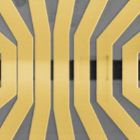
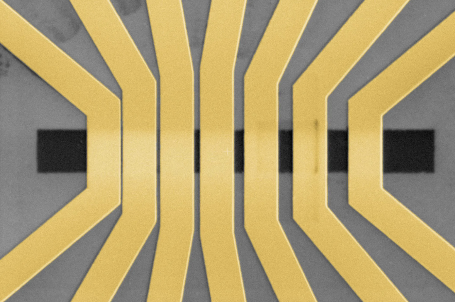
A test structure for determining the contact resistance between a 2D semiconductor and metal. | ARAVINDH KUMAR
In the quest to keep Moore’s Law going, you might imagine wanting to shrink transistors until the smallest part was just an atom thick. Unfortunately, that won’t work for silicon. Its semiconducting properties require a third dimension. But there is a class of materials that act as semiconductors even though they are two-dimensional. And new results from some of the biggest chip companies and research institutions show that these 2D semiconductors could be a good path forward once silicon’s limits are reached.
In work presented this week at IEEE International Electron Devices Meeting, in San Francisco, researchers at Intel, Stanford, and TSMC presented separate solutions to one of the most vexing barriers to making 2D transistors: sharp spikes of resistance at the places where the semiconductor meets metal contacts. Meanwhile, engineers at imec showed both how they’re clearing a path to commercial-grade manufacturing processes and demonstrating just how small future 2D transistors might be. And researchers in Beijing and Wuhan have constructed the 2D equivalents of the most advanced types of silicon devices.
“Silicon has reached its limit,” says Krishna Saraswat, a professor of electrical engineering at Stanford University. “People claim that Moore’s Law is over, but in my opinion that’s not the case. Moore’s Law can continue by going in the 3rd dimension.” For that, you need 2D semiconductors or something like them, says Saraswat, who collaborates with Stanford professors Eric Pop and H.-S. Philip Wong on 3D chips. Because of their potential to scale down to small size and relatively low processing temperatures, 2D semiconductors could be built in multiple layers.
Rival chipmakers TSMC and Intel separately hit on a different solution—antimony
Aravindh Kumar, a student of Saraswat’s, came up with one of a pair of solutions to the problem that were reported at IEDM. In prior research, gold had been the contact of choice for forming transistors with MoS2. But depositing gold and other high-melting-point metals damages the MoS2, making the barrier problem worse. So Kumar experimented with indium and tin, which have melting points in the low hundreds of degrees C.
Depositing gold disrupts the 2D semiconductor. But indium and tin do no damage. | ARAVINDH KUMAR
But those values are so low that these metals would melt during the latter parts of the chip processing and packaging process, which which exposes chips to temperatures reaching 300-500 degrees C. Even worse, the metals were oxidizing during processing. While trying to solve the latter problem, Kumar fixed the former. The answer was to alloy the low-melting point metals with gold. The indium or tin are deposited onto the MoS 2 first, protecting the semiconductor, then they are capped with gold to keep away the oxygen. The process leads to a tin-gold alloy with 270 ohm-micrometer resistance and indium-gold with 190 ohm-micrometer. And both alloys should be stable to at least 450 degrees C.
Rival chipmakers TSMC and Intel separately hit on a different solution—antimony. The idea is to reduce the energy barrier between the semiconductor and the contact by using a semimetal as the contact material, explains Han Wang, manager for low-dimensional research at TSMC Corporate Research. Semimetals, such as antimony, are materials that behave like they are at the boundary between a metal and semiconductor and have zero band gap. The resulting Schottky barrier is very low, leading to low resistance in both the TSMC and Intel devices.
TSMC had previously worked with bismuth, another semimetal. But its melting point was too low. Antimony’s better thermal stability means it will be more compatible with existing chipmaking processes, lead to longer-lasting devices, and allow for more flexibility in the latter part of the chip making process, says Wang, who worked with Stanford's Wong in the latter's role as TSMC chief scientist.
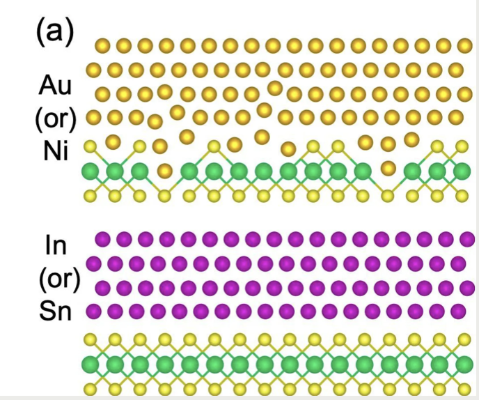
Besides making better devices, researchers at imec are interested in finding paths to integrating 2D semiconductors on commercial 300-mm silicon wafers, says Inge Asselberghs, program manager for exploratory logic. Using 300-mm wafers, imec to explore how small 2D devices might eventually get. Using tungsten disulfide as the semiconductor, the researchers formed double gate transistors, where the WS2 is sandwiched between top and bottom electrodes that control the current flowing through. Employing patterning tricks, they managed to scale down the top gate to below 5 nanometers. That particular device didn’t perform particularly well, but the research pointed toward ways to improve on it.
Separately, in research to be presented later this week, imec will show 300-mm compatible process optimizations steps to improve MoS2 transistor characteristic by including a gadolinium aluminate interlayer among other things.
Imec made a tungsten disulfide transistor with a gate length less than 5 nanometers. | IMEC
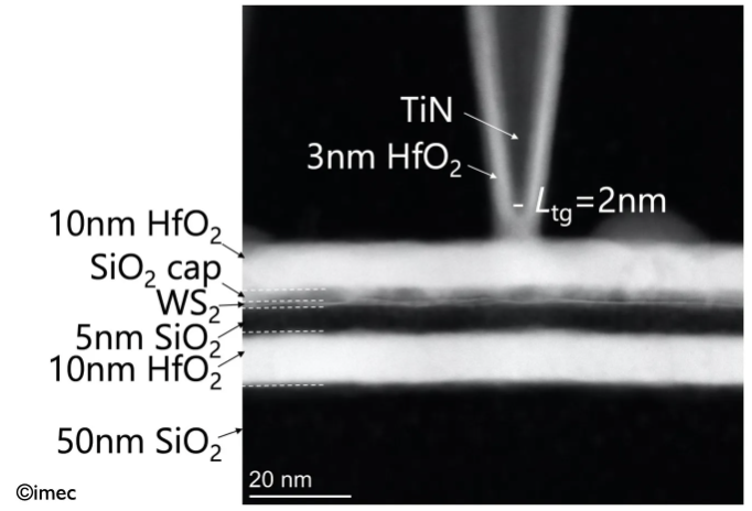
Though double-gate devices like imec’s are the norm for 2D research, engineers at Peking University, in Beijing, and at Wuhan National High Magnetic Field Center took things one step further. Today’s silicon logic transistors, called FinFETs, have a structure in which current runs through a vertical fin of silicon and is controlled by a gate that drapes over the fin on three sides. But, in order to continue to scale down the size of devices while still driving sufficient current through them, leading chipmakers are moving to nanosheet devices. In these, ribbons of semiconductor are stacked up; each is surrounded by the gate on all sides. Beijing researchers led by Yanqing Wu, mimicked that structure using two layers of MoS2. The device turned out to be more than the sum of its parts: Compared with their single-layer devices, the 2D nanosheets had better than twice the transconductance, meaning for a given voltage it drove more than double the current.
Intel simulated an even more extreme version of the stacked 2D device. Its researchers went with six layers of MoS 2 and only a 5-nanometer gate length, instead of the Beijing device’s two layers and 100 nanometers, respectively. Compared with a simulated silicon device of the same vertical height and with a 15-nanometer gate length, the 2D device packed in two more nanosheets and performed better. And all that was despite the fact that electrons travel more slowly through MoS2 than through silicon and that the contact resistances are much higher.
Wu and colleagues then took another step toward mimicking the near-future plans of silicon device makers. CMOS chips, by definition, are made up of pairs of N-MOS and P-MOS devices. As a way to cram even more devices into the same area of silicon, chipmakers want to stack the two types on top of each other instead of arranging them side-by-side. Intel demonstrated such a silicon device, called a complementary FET (CFET), at last year’s IEDM. Wu’s team tried the same by replacing one of the MoS2 layers in their stacked device with tungsten diselenide. Then, by modifying the connections between the source and drain, the 2D CFET became an inverter circuit, with essentially the same footprint as a single transistor.
There's obviously a lot of work to do before 2D semiconductors gain a spot in mass manufacturing, but with the progress made on contact resistance and the potential shown by the new experiments, researchers are hopeful.
This post was corrected on 14 December to clarify imec's research contributions.
2D Semiconductors Stalk Silicon at the Edge of Moore’s Law - by Samuel K. Moore - IEEE Spectrum - December 14, 2021