
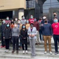
Prof. Srabanti Chowdhury leads the Wide-Bandgap (WBG) Lab at Stanford with a diverse and inter-disciplinary group of students and postdocs. The students in the WBG-Lab come from various backgrounds including in Mechanical, Chemical, Materials Science, and Electrical Engineering.
%202.jpg)
WBG-lab focuses on wide-bandgap semiconductors such as Gallium Nitride (GaN), Diamond, Gallium Oxide, and others in the family, to deliver innovative device technologies that can provide solutions for the growing demands for efficiency, versatility, compactness, and robustness in electronics. While most of today’s devices and gadgets have been made possible thanks to Silicon (Si), there is an increasing demand for more functionality and smaller footprint with lower losses, faster speed, and longer lifetime.
With the WBG materials, we are perfecting heterogeneously integrated solutions with Silicon to offer highly power-dense chips that can save energy consumptions. From micro-Grid to 5G-and-beyond, WBG materials are shaping the electronics, and we are thrilled to initiate some of those new research directions from our lab.
Our research, addressing some of the imminent global challenges in clean energy and wireless communication, starts with the synthesis of WBG materials. From fabricating devices to our design, characterizing their performance, all the way to demonstrating their potential in circuits, everything is done in the SNF, SNSF and the measurement labs located at AllenX. Our goal is to see WBG technology in action, and that’s exactly what our vertically integrated lab offers. We have the unique opportunity to experience the evolution of semiconductor device technology from its start to finish!
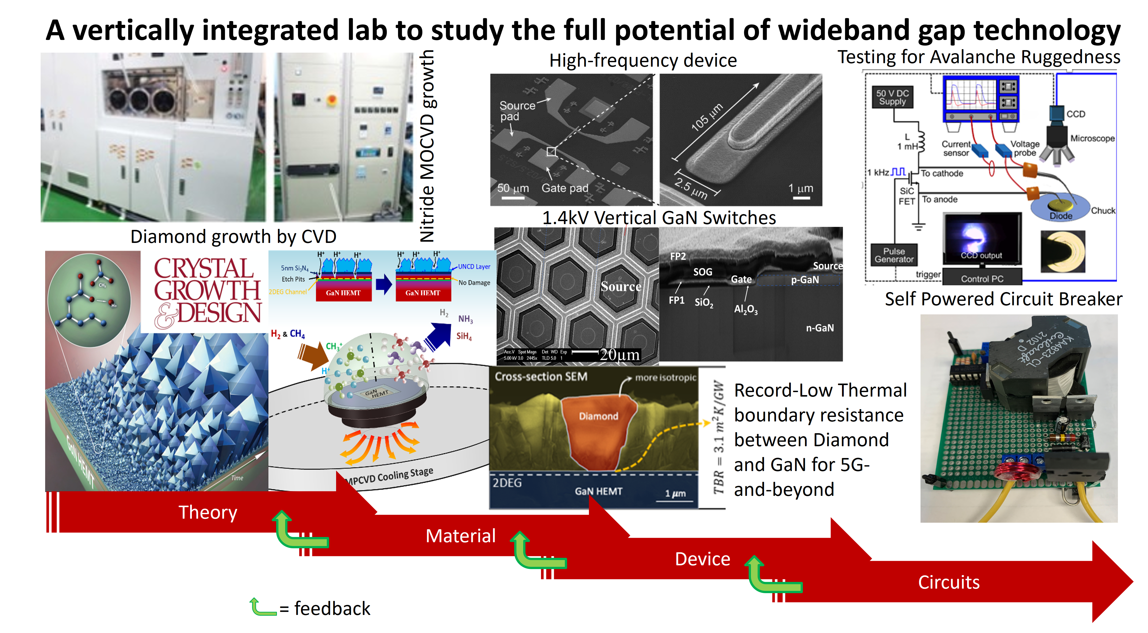
1. Starting from Materials
Nitrides: Every successful device technology stands on a strong material foundation. A significant part of our group focuses on studying the material growth/synthesis and their properties, producing some of the highest quality materials for device fabrication. High-performance devices such as the ones used for next-generation power electronics require epitaxial thin film growth using the metal-organic chemical vapor deposition (MOCVD) reactor (Figure 1). Two of our PhD students, Maliha Noshin and Jackson Meng, along with Dr. Kwangjae Lee are actively investigating techniques to perfect the GaN growth that would allow building high performing devices for power and RF electronics. Some of our recent work took shape during the pandemic where the epitaxial layers were manipulated with pores to emit green, yellow, and red light, only to be captured in a µ-LED!
Diamond: Working with Drs. Mohamadali Malakoutian and Rohith Soman, Ph.D. students Kelly Woo and Anna Kasperovich are looking into diamond aka the ultimate “ultra-wide-bandgap” semiconductors for its very large bandgap (~5x larger than Si!). Diamond has very high thermal conductivity and large voltage-handling (10’s of KV in a single device) properties, making it the ultimate choice for high-power electronics for future Electric Grids. As a heat spreader, diamond offers unrivaled prospects to improve performance all the way to the system level. Dr. Malakoutian, with a team of collaborators reported a record-low thermal boundary resistance of diamond when integrated with GaN, making it extremely attractive for 5G-and-beyond power amplifiers, where heat is a nuisance! We are also exploring diamond for thermal management of semiconductor integrated circuits using traditional Si and other III-Vs. Some of the fundamental work with diamond involves studying photo response in diamond as well as THz generation. We are actively focusing on electro-thermal solutions with diamond integration, achieved at low growth/deposition temperatures, to serve a wide range of applications, since heat is a problem in almost all electronics!
2. Materials to Devices
Novel device designs and engineering are the means to push the limits of performance, often beyond the material’s own limit! We have seen such examples in Si and now it is the time to bring those innovation to WBGs using GaN, Gallium Oxide, Diamond and Aluminum Nitride. Our Ph.D. students, Seungbin Jeong, Zhengliang Bian, Xinyi Wen, Adam F. Elwailly, Jeongkyu Kim along with Dr. Ke Zeng, are building novel devices in Nitrides, Oxides, or Diamond from scratch at the Stanford Nanofabrication Facility (SNF). One key area we focus on involves enabling avalanche rugged GaN power devices to bring unprecedented advantages in performance and reliability. They are exploring different types of vertical device technologies for power dense and reliable electronics that allows high-speed switching with lower energy. Diamond is being integrated to the chip to keep electronics ‘cool’ and efficient.
3. Device to Circuits
The bridge to circuit is often too far when you work with emerging materials and device technology. We are trying to build that bridge, looking from devices towards circuits. Modern wireless links 5G and beyond-5G use complex modulation schemes to achieve blazingly fast data rates at mm-Wave frequencies. However, achieving such a feat requires high RF output power to overcome the high path loss at these frequencies while at the same time preserving the characteristics of the signals being transmitted. Rafael Perez Martinez and Dr. Xinyu Zhou are working towards demonstrating the full scope of GaN device technology in RF applications.
With renewable energy sources, DC is gaining traction in data centers and residential settings due to its higher efficiency and lower operational cost. GaN-based power devices have tremendous potential in these DC power systems, especially in high-power DC-DC converters and self-powered DC circuit breakers. In particular, the normally-ON nature, ultra-fast switching speed, and low conduction losses make GaN HEMTs a very attractive choice for self-powered DC circuit breakers. Dr. Bhawani Shankar and Carla Pinzon are studying the circuit behavior of the devices that were built at the lab – starting from its very material synthesis.
Take a tour of the WBG Lab at Stanford University in the video below:
Lab Spotlight: WBeeGees at Stanford: Working with Semiconductors that Inspire! - by the WBG-Lab at Stanford - SystemX Alliance Newsletter - February 23, 2022
To view past newsletters, visit the SystemX Newsletter webpage.