
Core faculty: Jelena Vuckovic (EE), Shanhui Fan (EE), Hideo Mabuchi (AP), David A.B. Miller (EE)
Information processing systems are physically limited by both energy dissipation and communication of information, especially in dense, high-speed systems. Overall, the majority of energy dissipation in systems is in the interconnection and communication. Optics offers solutions to both of these problems, enabling lower energy communication and higher densities, especially for all longer distances beyond the chip itself. It also offers new possibilities for information processing at low or even essentially zero power.
New opportunities are emerging in optics for exploiting both multiple wavelengths and multiple spatial modes to allow us to continue to scale the information capacity of optical communications. These are enabled by a new generation of photonics that can be designed and customized to perform the exact function required. In turn, that photonics is physically enabled by emerging nanofabrication technologies, new complex nanophotonic structures, and by new fundamental understanding of optical components and design.
Additionally, advances in materials science and nanofabrication capabilities, combined with emerging new concepts in mesoscopic physics and quantum information theory are giving rise to a new field of study - quantum engineering. In essence, these developments in basic and applied science are creating new technological capabilities that could hardly have been foreseen during the formative years of electrical engineering. In order to facilitate the near-term realization of new quantum devices and systems, there is an immediate need to broaden the core analysis and design methodologies of electrical engineering to accommodate quantum substrates and quantum dynamical phenomena.
The goal of our focus group is to explore a number of topics in the areas of photonic and quantum technologies, with the goal to develop a new and a more efficient platform for computing and data processing. Below we outline several selected research tasks of our interest.
Dense highly-functional optics for interconnect and communication (lead: Miller)
We have recently understood that, if we can separate arbitrary overlapping beams, we can design any linear optical component [1]. Furthermore, in a significant intellectual breakthrough, we have understood that any such component can be designed, and we have at least one way of designing it [2]. In a second major advance, we have shown how such designs could even be self-configuring and self-stabilizing [2].
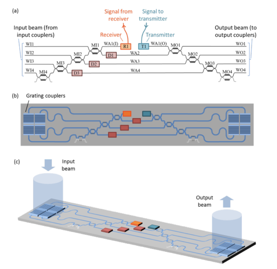
Figure 1. Spatial reconfigurable add-drop multiplexer. (a) Circuit schematic with integrated optics MachZehnder interferometer and mostly-transparent detectors. (b) A possibly layout suitable for silicon photonics. (c) A visualization of the device in use.
These realizations, combined with other optimized design approaches, mean we can now explore the next generation of optical technology, for high density, sophisticated optical systems, well beyond the complexities previously contemplated. This should allow new highly functional systems for communication using all the modalities that light offers, and the prospect of arbitrary linear processing and some nonlinear approaches that could relieve power dissipation in conventional approaches. For example, Figure 1 shows a concept for a spatial reconfigurable add-drop multiplexer that could loss-lessly extract a beam of a given shape from other overlapping beams, and then reinsert it with different information. We will explore the feasibility and capability of such approaches for this next generation of optics.
Aperiodic and dynamic nanophotonic structures (lead: Fan)
Future computing and communication systems require miniaturized components integrated into complex system for advanced information processing functionalities. The use of aperiodic and dynamic photonic structures will be playing very significant roles in meeting such requirements. In particular, the use of aperiodic structures enables the constructing of highly non-intuitive yet functional components at single wavelength scales. The use of dynamic structures provides reconfigurability, as well as functionalities that are not available in static systems such as dynamic non-reciprocity.
We have made significant advancements in developing an understanding of aperiodic photonic structures. A particularly important contribution is the developments of ultra-fast numerical algorithms that enable fast simulations and optimization of nanophotonic structures [3]. With these algorithms we are able to scan through very large ensemble of nanophotonic structures to develop a statistical understanding of these components in the presence of structural 3 variations, and to design highly functional and yet compact components for mode division multiplexing and wavelength division multiplexing systems.
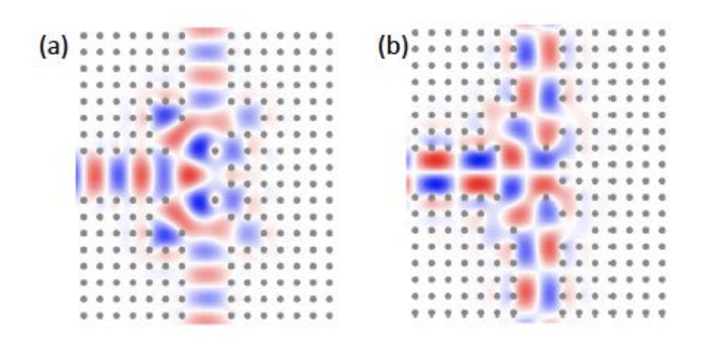
Figure 2. A mode splitter that preserves modal content.
We have also carried out significant works in the study of dynamic photonic structures. Here, a particularly noteworthy development is the recognition that dynamic refractive index modulation can be used to break time reversal symmetry, leading to non-reciprocal optical components that completely reproduce the effects of standard magneto-optics, but with materials that are entirely CMOS-compatible [4]. We have further shown that the phase of dynamic modulation becomes a gauge field for photons that provides tremendous flexibility for the control of flow of light [5,6].
In the next few years, we believe that the interplay between aperiodic and dynamic structures, will lead us to harness the complexity of nanophotonic structures both in the spatial and the temporal domain, leading to enhanced capabilities for manipulating light on chip.
Inverse nanophotonic design and implementation (lead: Vuckovic)
Remarkable progress has been made in optics (micro- and nano-photonics) over the past few decades, mostly focused around photonic crystals, quasi-crystals, and metamaterials. Despite such remarkable progress, all of the aforementioned structures are based on relatively simple geometries, consisting of regular shapes such as circles and rectangles, are periodic in two or three dimensions (photonic crystals and meta-materials) or in higher dimensions (quasicrystals). They are constructed by repeating a simple unit cell in space (real 3D space for photonic crystals and metamaterials, or higher dimensional space for quasicrystals). Therefore, such materials span only a very limited set of the possible parameter space for optical structures, and it is extremely unlikely that optimal designs are in such a limited sub-space. In other words, most (if not all) of the optical structures we have ever studied are not optimal.
We have recently developed a computational nanophotonic method (inverse design method), which is based on adapting the techniques of convex optimization to electromagnetics problems [7]. This approach enables us to optimize an optical device (structure) for a specific function without any restrictions on the parameter space. The optimized structures are free of any restrictions (such as periodicity in some number of dimensions or having to consist of regular 4 shapes), except for constraints possibly imposed by the designer resulting from the experimental capabilities, such as fabrication tools and the set of available materials. This method can be used to design a structure that converts a desired input field to desired output fields. The researcher only identifies the desired input and output fields, conversion efficiencies, footprint, and any desired frequency dependence of the device characteristics. The researcher can also specify constraints on materials and feature sizes, if any. The algorithm starts with a black box and slowly converges (by spanning the full parameter space) towards a solution that exhibits the desired behavior. Therefore, the full parameter space can be explored in this process. The optimal structures designed using this method outperform conventional photonic structures, and do not look like designs we have seen in photonics before, which have traditionally been designed by brute force parameter optimization and researcher intuition.
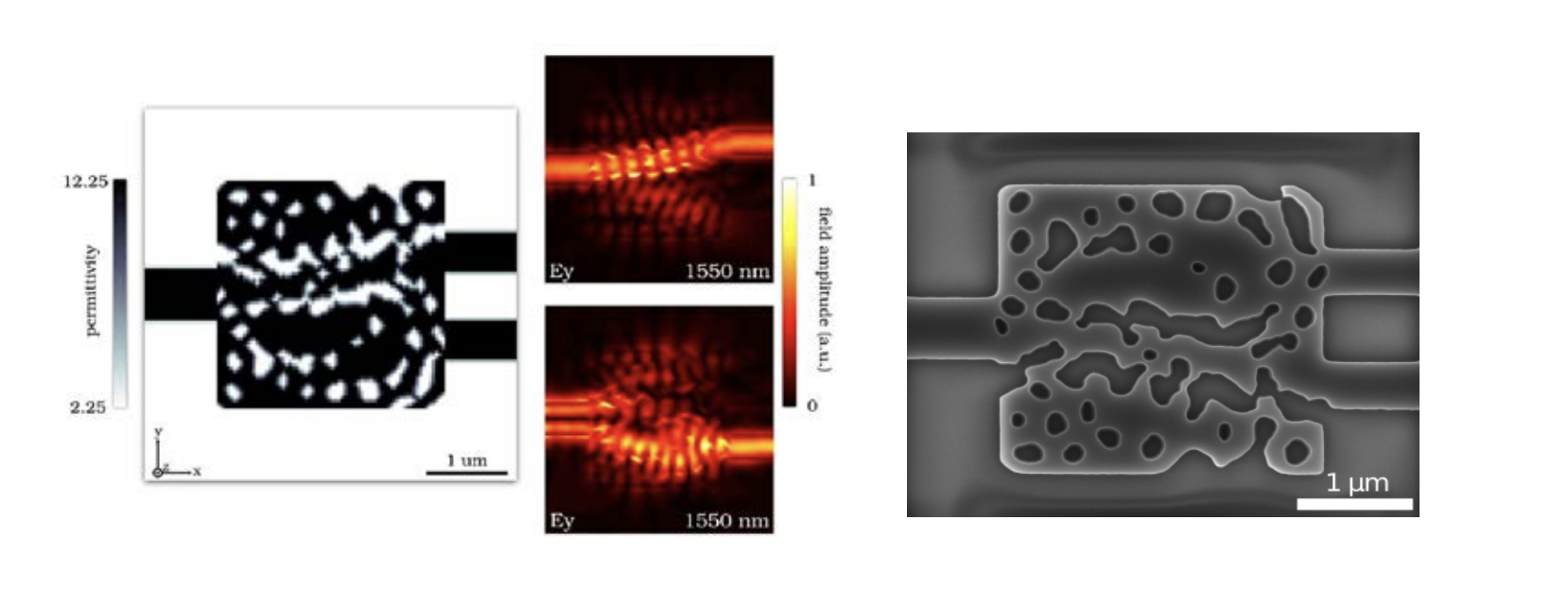
Figure 3. A compact spatial mode demultiplexer. Input mode is either the fundamental or second-order TE-polarized mode on the left. Output modes are the fundamental waveguide modes of either output waveguide on the right. Output power into the desired output arm is specified to be greater than 90%, while power into the opposing arm is set to below 1%. The fundamental mdoe is routed with nerly 100% efficiency to the top right output port, and the 2nd order mode is routed to the bottom right port. As a result of design, the conversion efficiencies into the upper and lower output arms are 88.7% and 77.4% respectively, while the rejection powers for the same modes are 0.27% and 0.20%. Device footprint is 2.8 × 2.8 microns. The designed structure is based on silicon on insulator, 200nm thick slab, and has fabricable features. The fabriucated structure is shown on the right (mirror image of the design).
Using our inverse design algorithm, we have designed a wide variety of linear waveguide-based nanophotonic devices such as wavelength splitters, spatial mode multiplexers, TE/TM splitters, waveguide crossings, and fiber couplers [7]. These nanophotonic structures are fully three-dimensional and multi-modal, have very compact footprints (a few microns long at most), exhibit high efficiency, and are manufacturable. One of these devices, a spatial mode demultiplexer, is presented in Figure 3. We have also experimentally demonstrated some of these structures [8], showing that our inverse designed structures can be fabricated and are robust to fabrication imperfections.
Our goal in the next few years is to expand this design process from designing individual optical devices and components to design of functional photonic circuits for applications ranging from optical interconnects to image processing.
Algorithms and Software for Quantum Engineering (lead: Mabuchi)
Although much is known about the device physics of individual quantum components in the optical and superconducting (microwave) settings, there is a significant gap in our base of concepts, algorithms and software tools for modeling and analyzing complex networks of such components, i.e., quantum photonic circuits. Recent theoretical advances in the area of quantum stochastic differential equations have provided the rigorous basis for the interconnection of quantum input-output models of individual components to obtain quantitative models for the dynamics of whole circuits, including the possibility of external driving fields and physically realistic models of decoherence.
With the ultimate goal of making this advanced capability accessible to practicing electrical engineers and computer architects, we have begun to develop a modeling/simulation workflow and associated software tools that we collectively refer to as the Quantum Hardware Description Language (QHDL) paradigm. In our approach [9], one can use existing circuit layout software (such as gschem) to construct the netlist for a quantum photonic circuit by drawing components from a special library of quantum optical devices that we provide as part of our QNET software bundle (mabuchilab/QNET on GitHub). The netlist can be saved in the standard VHDL format and our software “compiles” this netlist into a quantum field-theoretic model of the circuit dynamics, in the form of a master equation or equivalent description (quantum trajectory model, Heisenberg equations, etc.). We are developing post-processing tools that implement various model reduction methods that simplify the computational complexity of simulating these circuit models in appropriate parameter regimes. A number of research papers have already been published on the QHDL paradigm and its applications, and we and other research groups have begun to investigate extensions of QHDL to incorporate superconducting electrodynamics and opto-mechanical components.
The current version of the QHDL software suite targets workstation and small server architectures, which limits the size/complexity of circuits that can be studied. Restructuring the code for HPC platforms will make it possible to model large quantum networks of interest for strategic applications. The impact of the QHDL tool suite can be further amplified by the addition of new modules that go beyond circuit simulation and analysis to address quantum network design. Taking this step will require the development of new circuit design methods and computational algorithms to implement them.
While we have a number of ideas on quantum photonic circuit design methodology [10], we have not yet begun to consider how any of these methods could best be implemented in practical software tools. Of course, computational efficiency will be a primary consideration in determining which specific design methods are most promising for continued study.
Affiliated faculty
Our focus group also includes a number of affiliated faculty for a range of engineering and science departments at Stanford: Jennifer Dionne (MSE), Martin Fejer (AP), David Goldhaber Gordon (Ph), Benjamin Lev (AP), Kam Moler (AP-Ph), Amir Safavi-Naeini (AP), Monika Schleier-Smith (Ph).
References
[1] D. A. B. Miller, "All linear optical devices are mode converters," Opt. Express 20, 23985- 23993 (2012)
[2] D. A. B. Miller, "Self-configuring universal linear optical component," Photon. Res. 1, 1-15 (2013).
[3] V. Liu, D. A. B. Miller and S. Fan, “Application of computational electromagnetics for nanophotonics design and discovery”, Proceedings of the IEEE, vol. 101, no. 2, pp. 484-493 (2013).
[4] Z. Yu and S. Fan, “Complete optical isolation created by indirect interband photonic transitions”, Nature Photonics, vol. 3, pp. 91-94 (2009).
[5] K. Fang, Z. Yu and S. Fan, “Realizing effective magnetic field for photons by controlling the phase of dynamic modulation”, Nature Photonics, vol. 6, pp. 782-787 (2012).
[6] L. Tzuang, K. Fang, P. Nussenzveig, S. Fan, and M. Lipson, “Non-reciprocal phase shift induced by an effective magnetic flux for light”, Nature Photonics, vol. 8, pp. 701-705 (2014).
[7] Jesse Lu and Jelena Vuckovic, “Nanophotonic computational design,” Optics Express, 21 (11), pp. 13351-13367 (2013)
[8] Alexander Y. Piggott, Jesse Lu, Thomas M. Babinec, Konstantinos G. Lagoudakis, Jan Petykiewicz, and Jelena Vuckovic, “Inverse design and implementation of a wavelength demultiplexing grating coupler,” Scientific Reports 4, 7210 (2014)
[9] N. Tezak, A. Niederberger, D. S. Pavlichin, G. Sarma and H. Mabuchi, “Specification of photonic circuits using Quantum Hardware Description Language,” Phil. Trans. Roy. Soc. A 370, 5270 (2012).
[10] D. S. Pavlichin and H. Mabuchi, “Photonic circuits for iterative decoding of a class of low-density parity-check codes,” New J. Phys. 16, 105017 (2014).
Focus Area Lead
 |
Prof. Jonathan FanElectrical Engineering |